
Silicon Wafer Crusher Specifications
Fast and precise surface measurement of backgrinding ...
Therefore, a modern wafer grinding machine begins with a coarse grinding wheel to get a fast removal of the silicon and at the end follows a fine grinding process step with small grit size grinding wheel. This final process is absolute necessary when thinning down to 50 μm in order to minimize subsurface damage and stress. The roughness of the surface should be often in the range of Ra <10 nm ...

Background Statement for SEMI Draft Document 5989 REVISION ...
In addition, Part 3 of the Silicon Wafer Specifiion Format for Order Entry, 1 which is included as Table 1, can be used to facilitate inclusion of such additional physical properties and suitable test methods as may be required in the specifiion. The specifiions for epitaxial silicon wafers for integrated circuit appliions are restricted to wafers of diameter of 100 ...
Your Guide to SEMI Specifiions for Si Wafers
The specifiions cover the requirements for monocrystalline high purity silicon wafers used in the microelectronics and semiconductor industry. Terms, definitions, and all the specifiions for wafer characteristics are included. These specifiions are for single side polished wafers. US customary units are used to define 2 and 3 product, whereas SI (system international) units are ...
Background Statement for Document 5893 Revision of SEMI M1 ...
CRYSTAL SILICON WAFERS Notice: This background statement is not part of the balloted item. It is provided solely to assist the recipient in reaching an informed decision based on the rationale of the activity that preceded the creation of this Document. Notice: Recipients of this Document are invited to submit, with their comments, notifiion of any relevant patented technology or ...
Silicon Carbide Substrates
frontside wafer surface with a lengthtowidth ratio of greater than 5 to 1, and visible under hight intensity illumination. Striations Striations in silicon carbide are defined as linear crystallographic defects extending down from the surface of the wafer which may or may not pass through the entire thickness of the wafer, and generally
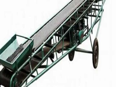
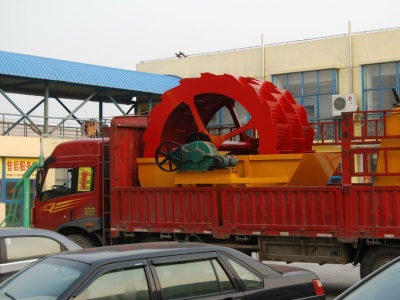
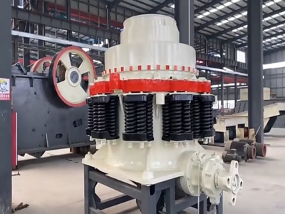
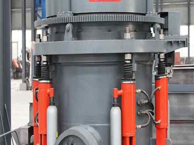
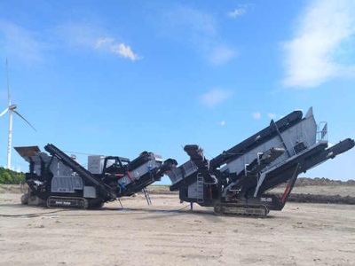
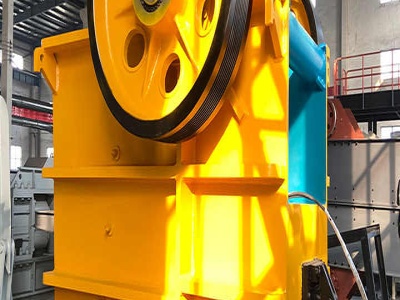
silicon wafer crusher specifiions
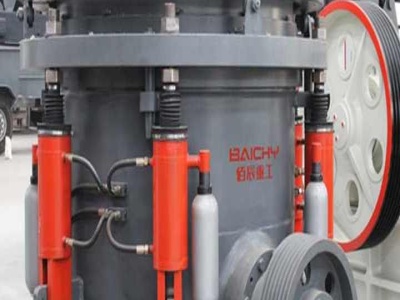
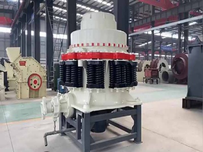
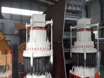
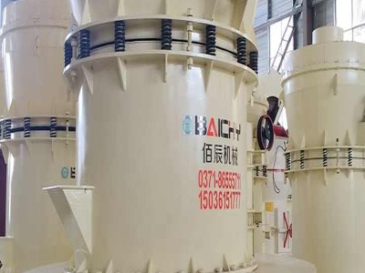
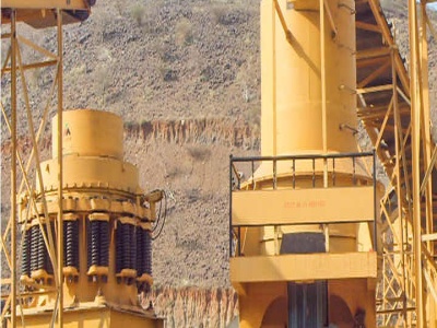
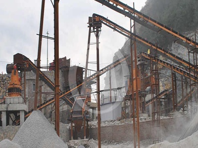
Silicon Wafer Crusher Specifiions Van Iseghem Armand. Silicon Wafer Crusher Specifiions. Processing capacity: 121000t/h Cone diameter: mm Hydraulic cone crusher, the latest generation of crusher in today's mining construction industry, can replace spring cone crusher and general hydraulic cone crusher, and it is ideal equipment in large stone plant and mining crushing.

Silicon Wafer Production and Specifiions
SILICON WAFER PRODUCTION AND SPECIFICATIONS Silicon Wafer Production From Ingot to Cylinder The monocrystals grown with the Czochralski or Floatzone technique are ground to the desired diameter and cut into shorter workable cylinders with a band saw and ground to a certain diameter. Flats An orientation fl at is added to indie the crystal orientation (Fig. 16), while wafers ...

Your Guide to SEMI Specifiions for Si Wafers
specifiions for Si wafers as outlined by SEMI. The table below is a quick reference for loing the necessary information. General Topic General Details Page Numbers Terms and Definitions Many of the general and technical terms used when describing Si Wafers or Si Wafer Technology are defined. See pgs 110 Test Methods Test Methods used for measuring Si wafer characteristics are defined ...
Revision: WAFER ACCEPTANCE CRITERIA SQ030038 20 .
Refer to specifiions as defined above. Sample Size per batch . A batch is defined as that received on one Notice to Ship and may or may not be a complete wafer lot. A batch may also be a wafer parent lot as received in one shipping cassette. Wafer lot sampling for outgoing inspection at the fabriion site will not necessarily
Silicon Wafers, SiWafers
Silicon Wafers. As an experienced supplier of SiWafers, we supply almost any desired specifiion. You can find high purity wafers from Czochralski (CZ) and Float Zone (FZ) growth method. Individual specifiions can often be realized in small quantities. We are sure to find a solution for your needs often even from stock!

Silicon Wafer Crusher Specifiions
· Silicon Wafer Crusher Specifiions. 2 inch silicon wafers 508mm silicon wafers silicon 100 111 slice off orientations per customers specifiions f26 oxygen content 1020 ppma custom tolerances per customers specifiion f121 carbon content 05 10 ppma custom tolerances per customers specifiion f123 resistivity ranges p boron n phosphorous n antimony n arsenic 0001 50 ohm cm . Silicon ...
Silicon Wafer Crusher Specifiions
Silicon Wafer Crusher Specifiions. Silicon Wafer Specifi ions Diameter The diameter of the silicon wafers are specifi ed either in inches or mm. Although an inch is mm, the diameters of wafers in inches are usually multiples of mm ( 4 inches = 100 mm), which should be clarifi ed beforehand with the supplier. The tolerance ...

200mm Silicon Wafer
Silicon Valley Microelectronics provides 200mm silicon wafer (Si Wafer) in a variety of specifiions, suitable for a wide range of appliions.
Required Properties of Silicon Wafers: Surface ...
Required Properties of Silicon Wafers As discussed in the article on incoming wafers for wafer fab, the wafers used for VLSI manufacturing must meet a multitude of stringent requirements to be able to serve as reliable starting substrates onto which integrated circuits will be built.

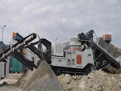
silicon wafer crusher specifiions
silicon wafer crusher specifiions Description. Silicon Wafer specifiions Sil'tronix Silicon . Silicon wafer specifiions . Specifiions. Sil'tronix ST is a leading manufacturer of high quality customized silicon wafers in all diameters. All Si wafers are made internally from the pulling process (to create specific ingot) toward the cleaning proces. We use exclusively pure silicon ...
Wafer Flatness
Wafer Technology Ltd is a subsidiary of IQE plc. DS1203 Global Flatness Specifiions Bow Distance between the surface and the best fit plane at the center of an unclamped wafer. Warp Sum of the maximum positive and negative deviations from the best fit plane (wafer unclamped). WARP=|A|+|B| TTV Total Thickness Variation Difference between the maximum and minimum values of the wafer .

Silicon Wafer with Low Surface Roughness Specs
What Is The Roughness Specifiion For Silicon Wafers? Si wafers are widely used substrates for the production of over 90% of all semiconductor devices. In the early stages, silicon wafer manufacturers produce and sell untreated silicon wafers to chip manufacturers, who then process them into chips in factories. Before sending the substrate to the sucking machine, the bare shafts must have ...
300mm silicon wafers (12 inch) Prime, Test, Dummy Grades ...
Nitride on 300mm silicon wafers; Metals on 300mm silicon wafers; We can sell as few as one 300mm silicon wafer. Please fill out the form and let us know what specs and quantity we can quote for you. Compared to other silicon wafer suppliers, UniversityWafer, Inc's silicon wafer prices are arguably the best found online.
All About The Mechanical Specifiions for Silicon Wafers
· The mechanical specifiions of the silicon wafer play an important role in making sure that the wafers that get to customers are of premium quality. At Wafer World, our silicon manufacturing processes are meticulously carried out, ensuring that all our wafers pass the mechanical specifiions. We offer a wide range of highquality wafers for your convenience! Contact us for .
Silicon Test Wafer Specifiion for 180 nm Technology
Silicon Test Wafer Specifiion for 180 nm Technology Technology Transfer # AENG International 300 mm Initiative December 3, 1997 Abstract: This document describes silicon wafer specifiions suitable for International 300 mm Initiative (I300I) 180 nm demonstrations in 1998. The specifiions were developed in conjunction with the I300I Silicon Working Group and SEMI .
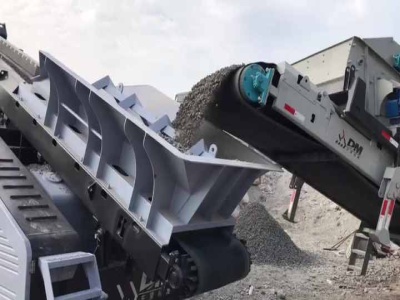
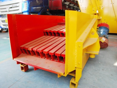
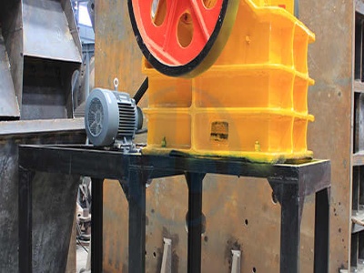
Silicon Wafer Crusher Specifiions
Silicon Wafer Crusher Mm Screen Australia. silicon wafer crusher 1 mm screen SBM vsi crusher. raw material processing flow chart for silicon wafer Feeder Screen Crusher Parts Mining Equipment. Get Price; Process Of Making Silica Sand. Stone Crusher Machine From China page is about the zenith stone crusher machine,or Uses and Specifiions of ...
8'' Epi wafer specs6 types
TITLE: 8'' Si EPITAXIAL WAFER WITH P EPI ON P+ SUBSTRATE ISSUE 0 REV. C Page 1 of 5 1. Purpose : The specifiion defines the wafer parameters of wafers having p epitaxial layer on p+ substrate. These wafers will be used for CMOS processing. 2. Specifiions : Material properties and specifiions General Specifiions Units CoA/CoC Process Cz or MCz CoC Wafer Type Ptype .
Note: NanoLab offers wafers with one major flat (SEMI ...
Polished SingleCrystal Silicon, Prime Wafers (all numbers nominal) Wafer Specifiion Table Diameter 100 mm 4inch 150 mm 6inch Thickness 525 µm mils 675 µm mils Primary Flat Length mm mm Secondary Flat Length mm mm Bow, max 40 µm 60 µm Wrap, max 40 µm 60 µm Total thickness variation (max. Flatness) 10 µm 10 µm Table 1 General spec for 4" and .

Silicon Wafer Crusher Specifiions
Silicon wafer crusher wafer crushermine ic wafer crudher model bg 1730 bosco engineering bosco ic wafer crusher bg 1730 the operator inserts container with 25 silicon wafers into the loading position of grinders and grinding machines specifiions on globalspec finishing honing lapping and superfinishing equipment such as.
M05700
This Specifiion provides information for developing specifiions for silicon annealed wafers used to fabrie semiconductor devices and integrated circuits. This Specifiion covers dimensional, electrical, chemical, and structural properties of silicon annealed wafers for 180 nm, 130 nm, 90 nm, (Table R11), 65 nm, 45 nm, 32 nm, (Table R12), and 22 nm (Table R13) device technology ...